Semi Conductor
Semi Conductor
aNexus High-Precision Electron Beam Lithography (EBL) System for Advanced Semiconductor & Quantum Research
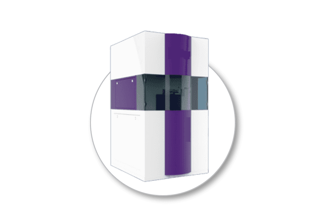
Our Electron Beam Lithography (EBL) System is engineered for high-resolution, high-speed patterning on semiconductor wafers, making it ideal for cutting-edge research and industrial applications across Southeast Asia.
Equipped with a field emission gun (FEG) and a built-in high-speed graphics generator, this advanced EBL tool enables ultra-precise lithography at nanometer scales. It features a laser interferometer-based motion stage, delivering exceptional accuracy in large-area patterning, high-precision stitching, and overlay alignment, essential for next-generation device fabrication.
This EBL system supports a wide range of innovation-driven industries, including:
- Semiconductor manufacturing
- Microelectronics and photonics
- Quantum computing and nanotechnology
- Advanced materials development
- Fundamental and applied physics research
Key Features of the Electron Beam Lithography (EBL) System
1. Advanced Laser Interferometer Stage
Our EBL system is equipped with a high-precision laser interferometer stage designed for large-stroke movement, delivering exceptional accuracy in stitching and overlay alignment. This ensures reliable pattern placement across a wide writing area—ideal for advanced semiconductor and nanofabrication applications.
2. High-Resolution Field Emission Gun (FEG)
At the core of the system is a high-resolution field emission gun, which provides a stable, focused electron beam—critical for achieving superior lithography quality and consistent pattern fidelity, even at nanometer scales.
3. Ultra-High Resolution with High-Speed Scanning
Engineered for both ultra-high resolution patterning and ultra-fast scanning speeds, this system enhances throughput without compromising accuracy. It is an optimal choice for institutions and manufacturers working on next-generation microelectronics, photonic devices, and quantum research.
Stage Specifications
| Standard Equipment | Laser Interferometer Stage |
| Stage Travel | ≤105 mm |
Electron Gun and Imaging Specifications
| Schottky Field Emission Gun | Acceleration Voltage 20V ~ 30kV; Side Secondary Electron |
| Image Resolution | Detector and In-Lens Electron Detector |
| Beam Current Densit | > 7000 A/cm² |
| Minimum Beam Spot Size | ≤2 nm |
Lithography Specifications
| Electron Beam Shutter | Rise Time < 100 ns |
| Writing Field | ≤500×500 um |
| Minimum Single | < 15 nm (dependent on process conditions) |
| Exposure Line Width | ≤20 MHz |
Graphics Generator Parameters
| Control Core | High-performance FPGA | Minimum Dwell | 10 ns |
| Maximum Scan | 50 MHz | Time Increment | GDSII、DXF、BMP, etc. |
| Speed | 20-bit | Faraday Cup Beam | Included |
| D/A Resolution | 10 um~500 um | Current Measurement | Optional |
| Supported Writing | 5 V TTL | Proximity Effect | Optional |
| Scan Modes | Sequential (Z-type), Serpentine (S-type), Spiral, and other vector scan modes | ||
| Exposure Modes | Supports field calibration, field stitching, overlay, and multi-layer | ||
| External Channel | automatic exposure | ||
Optional Accessories
-Companion UPS (Uninterruptible Power Supply)
-Companion Active Vibration Isolation Table, with a minimum natural frequency of 2Hz